flat panel displays that emit light in response to an electric current
Introduction
The two main ways of producing light are incandescence and luminescence. While in incandescence an electric current is driven through a conductor, which produces heat in resistance to the current and hence generates light, luminescence is generally referred to all forms of visible light due to other causes than temperature.
Electroluminescence (EL) thus means the non-thermal creation of light resulting from the application of an electrical field to a substance. The light-emitting substance is usually a doped luminescent crystal (phosphor), e.g. zinc sulfide (ZnS). Depending on the dopant, different colors can be achieved. The best results are achieved from a manganese-activated zinc sulfide (ZnS:Mn), which emits a yellow-orange color peaking at 585nm. A greenish light can be produced using a copper dopant (ZnS:Cu) and a silver dopant (Zns:Ag) will result in a bright blue.
The main types of electroluminescence are injection EL and high-field EL.
- Injection EL is the basic principle behind light emitting diodes (LED) technology. It results from a semiconductor p-n junction being biased in the forward direction and connected to a source of DC voltage. In this case either excess holes are injected into the n-region or excess electrons into the p-region. Luminescence occurs when the electrons and holes recombine. [1]
- High-field EL represents the functioning principle behind EL displays (ELD) and is produced by impact excitation of a luminescent center by high-energy electrons. ELDs are a type of flat panel display produced by sandwiching a light-emitting substance between two conductors. They are extremely rugged, relatively insensitive to ambient temperature, exhibit rapid display response (<1ms), require very little current and emit a soft, perfectly homogenous light, which is visible from great distance and essentially unlimited viewing angle. They are compact, lightweight, inexpensive in production and can be made in any color. The light output of ELDs is very reliable with typically only 10% loss after 10.000 hours of operation and a lifetime of over 100.000 hours.
A white EL sheet being folded
History
The phenomenon of electroluminescence was first discovered by Captain Henry Joseph Round in 1907, when running current through a silicon carbide (SiC) detector. The next reported observation was in 1923, when Russian scientist Oleg Lossev confirmed the occurrence of yellow light-emission in SiC crystals. In the late 1920s Bernhard Gudden and Robert Pohl conducted experiments in Germany with copper doped ZnS. However it was not until 1936 when Georges Destriau, an associate of Marie Curie, discovered high-field EL and hence officially coined the term electroluminescence. [2]
During World War II a serious amount of research was performed on luminescent crystals in combination with radar displays but only in the 1950s companies like GTE Sylvania focused on powder EL phosphors and started developing the technology for practical applications. Nataliya Vlasenko and A. Popkov successfully fabricated the first thin-film EL (TFEL) structures in 1958 while observing that luminance was much higher when doping zinc with manganese (ZnS:Mn) as opposed to previously used copper (ZnS:Cu).
Despite continuous progress in EL technology the devices remained too instable for commercial use, until research revived in the mid 1960s with a focus on display applications. In 1965 Sigmatron Corporation demonstrated a TFEL dot-matrix display and in 1968 Aron Vecht developed DC EL technology to be used in lamps and watches. In 1974 Toshio Inoguchi at Sharp Corporation introduced an AC TFEL approach, which became the first high-brightness long-life ELD and kept Sharp at the leading edge for the following few decades. In the 1980s Christopher King developed advanced TFEL displays and launched Planar Systems in the US in 1983. Both companies, Sharp and Planar Systems, produced monochrome EL displays that were applied in early laptop computers since 1985.
In 1993, based on research by William Barrow and his team at Planar, the production of full-color Active Matrix EL (AMEL) microdisplays began. In the 1990s Xingwei Wu at Canadian company iFire developed thick-film dielectric EL (TDEL) technology. TDEL is based on inorganic EL technology and is brighter, more efficient, and more resistant to contamination during fabrication and to electrical breakdown than TFEL. Some TDEL use two layers of phosphors. The thick bottom layer is resistant to dielectric breakdown and can withstand a higher current to produce brighter light, while the upper layer consists of colored phosphors. Through this RGB EL devices can be created.
Mid 2007 Planar presented a transparent and segmented EL (TASEL) display in custom forms and sizes with curved and moldable shapes. [3] TASEL displays are based on the standard EL device structure but a transparent electrode replaces the metal rear electrode. [4] In 2012 Sung Hwan Cho et al. demonstrated a hybrid AC EL (HACEL) device containing a thin organic/inorganic nanocomposite film of Quantum Dots blended in a light emitting polymer matrix. The device exhibits high brightness and is supposed to overcome prevalent limitations in color blending and tuning. [5]
Device Structure and Operation
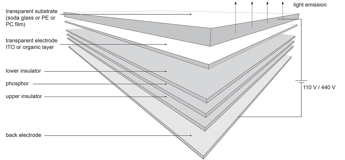
The supporting substrate of a TFEL display is usually made of very low sodium glass (1), coated with a transparent conductor such as indium tin oxide (ITO). In order to produce flexible displays a transparent PE or PC film can also be used as base substrate. The ITO layer is between 120 and 350nm in thickness (2). On top of the ITO a lower insulator (200nm) is deposited. The light emitting phosphor (4) is typically 200 – 1000nm in thickness and sandwiched between two insulating films (3, 5). [6] Due to the very high field level (1.5MV/cm) that is necessary to excite the phosphor layer to emit light, any defect in the thin-film stack could produce a short circuit and destroy the device. Hence current-limiting layers (the insulators) on both sides of the phosphor are essential. [7] The upper electrode is deposited on top of the upper insulator and is generally 100 – 200nm thick (6).
EL device structure
Luminance / voltage ratio
In most EL tape configurations, power is provided through copper or aluminum conductors. In EL sheets or panels different conductive materials can be used, depending on the design requirements. If an imaging matrix is desired, both electrodes are made of grids of parallel lines, with their orientations being orthogonal to each other. Using approximate circuitry the whole matrix can thus be scanned and voltage applied to any phosphor element that is located at the respective intersections.
Depending on the size of the TFEL device, it can be powered from a (small) inverter, which transforms low DC voltage to the appropriate level of AC power, causing an electric field to occur in between the upper and lower electrode. During each half-cycle electrons are emitted into the high-field region and get accelerated to ionize atoms of the crystal lattice. The resulting holes are trapped by luminescent centers. When the field is oriented into the opposite direction, due to the AC current, the electrons return to the luminescent centers, where they recombine with the holes to glow. The brightness of the display can be adjusted by controlling the frequency and voltage of the power supply. At low voltage it emits little or no light and acts like a pure capacitor. Once the voltage reaches a certain threshold value, determined by the dielectric properties of the insulating and phosphor layers, the brightness increases abruptly and steeply (6 lumens/watt) until it reaches a saturated region, where efficiency goes down (3lm/W). The relative brightness of a TFEL is roughly proportional to the driving frequency. Exceeding the maximum voltage and frequency of a TFEL might significantly reduce its lifetime.
Fabrication
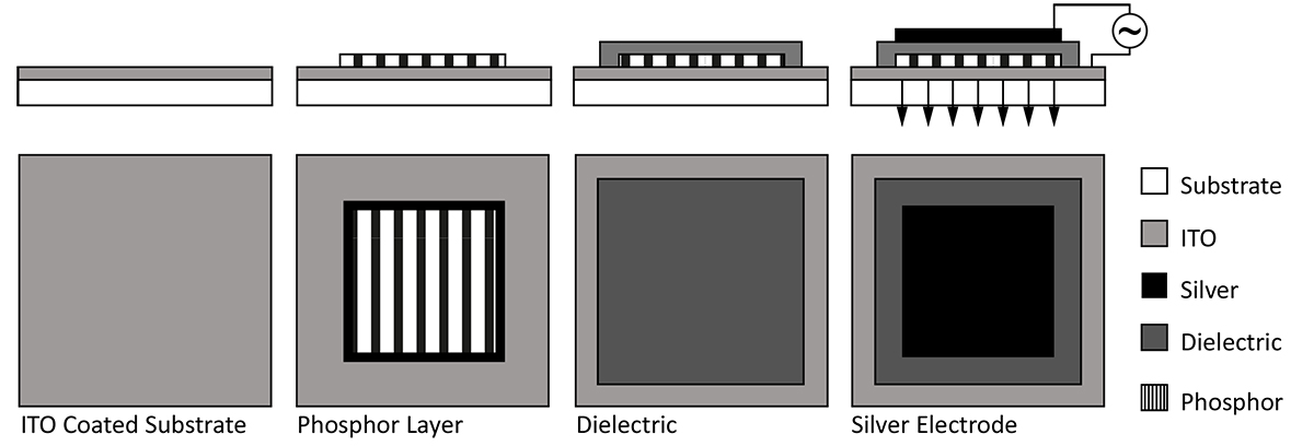
TFEL displays are commercially produced using a number of different deposition techniques. The electrode materials ITO and aluminum are often deposited by sputtering or physical vapor deposition (PVD). The insulator and phosphor layers are usually made by chemical vapor deposition (CVD) or PVD. EL displays can however also be fabricated using screen-printing techniques, which allow a great reduction in material usage, less costs and bring speed and adaptability to the fabrication process. [8] In screen printing the display consists of four layers:
1. A transparent conductive layer, which is either an ITO coated glass substrate or polyester film.
2. The phosphor layer has to be evenly spread across the electrode.
3. The thickness of the dielectric insulator layer depends on the insulating requirements. Usually this step is printed at least twice.
4. The rear electrode needs to match the inner edge of the bus bar and can either be silver or carbon ink.
The electric field is created across the phosphor by applying an AC voltage from the transparent conductive layer to the silver layer. [9]
EL screen-printing steps. (c) John Sarik.
Applications
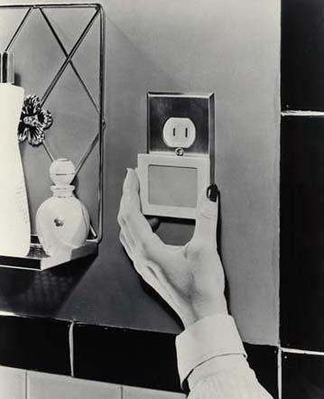
EL displays are used in a wide variety of applications. Already in the 1960s they have been produced as nightlights, display-keyboard interfaces or automotive panel backlighting. Today they are made to illuminate liquid crystal displays (LCD), advertising boards or safety-related products. As consumer materials they can be obtained in the form of EL strips, cables/wires, inks or films/sheets. In an architectural application they first emerged in 1957 as luminous surfaces in a model room. [10] Currently they are being applied as luminescent floor or wall coverings or large format displays in public spaces. Various artists have experimented with EL surfaces, including Dutch designer Jonas Samson, who developed electroluminescent wallpaper that can display simple animations or London based Loop.pH design studio whose “Blumen” project features floral patterns printed on a textile base to be used as spatial dividers. In Santiago Calatrava’s Opera House in Valencia EL films are integrated into the seating as background illumination and emergency guidance. [11]
References
[1] Ono, Yoshimasa A. 1995. Electroluminescent displays. Singapore: World Scientific, 1.
[2] Hart, J. A., Lenway, S.A., and Murtha, T.: A History of Electroluminescent Displays. (University of Minnesota: September 1999), 2.
[3] Abileah, A., Harkonen, K., Pakkala, A., and Smid, G., “Transparent Electroluminescent (EL) Displays”, 2008, 6.
[4] Antikainen, M., Haaranen, J., Honkala, J., Lahonen, M., Liias, V.-M., Pakkala, A., Pitkänen, T., Soininen, E. and Törnqvist, R. (2000), 34.2: Invited Paper: Transparent Emissive Thin-Film Electroluminescent Display. SID Symposium Digest of Technical Papers, 31: 885.
[5] Cho, S. H., Sung, J., Hwang, I., Kim, R. H., Choi, Y. S., Jo, S. S., Lee, T. W. and Park, C. (2012), High Performance AC Electroluminescence from Colloidal Quantum Dot Hybrids. Adv. Mater., 24: 4545.
[6] Barrow, William A. 1999. “Electroluminescent displays”. The Measurement, Instrumentation and Sensors Handbook / Editor in Chief John G. Webster, 2.
[7] King, C. N. (1996), Electroluminescent displays. Journal of the Society for Information Display, 4: 1–8. doi: 10.1889/1.1984982, 1.
[8] Michael Brunner ; Thomas Welker; Electrical and optical properties of screen-printed electroluminescent structures. Proc. SPIE 5632, Light-Emitting Diode Materials and Devices, 324 (January 19, 2005), 324.
[9] Sarik, J.; Akinwande, A.I.; Kymissis, I., “A Laboratory-Based Course in Display Technology,” Education, IEEE Transactions on , vol.54, no.2, pp.314,319, May 2011, 315.
[10] Ritter, Axel. 2007. Smart materials in architecture, interior architecture and design. Basel: Birkhäuser, 132
[11] Sauer, Christiane. 2010. Made of –: new materials sourcebook for architecture and design. Berlin: Gestalten, 166.


