screen-printing light-emitting foils
The fabrication process was adapted from the Columbia University course Modern Display Science and Technology, which was developed by researchers at the Columbia Laboratory for Unconventional Electronics (CLUE). CLUE uses thin film materials and low temperature fabrication techniques to build sensors, displays, and other electronic devices on unconventional substrates. This novel integration enables the creation of large, flexible, non-planar electronic systems.
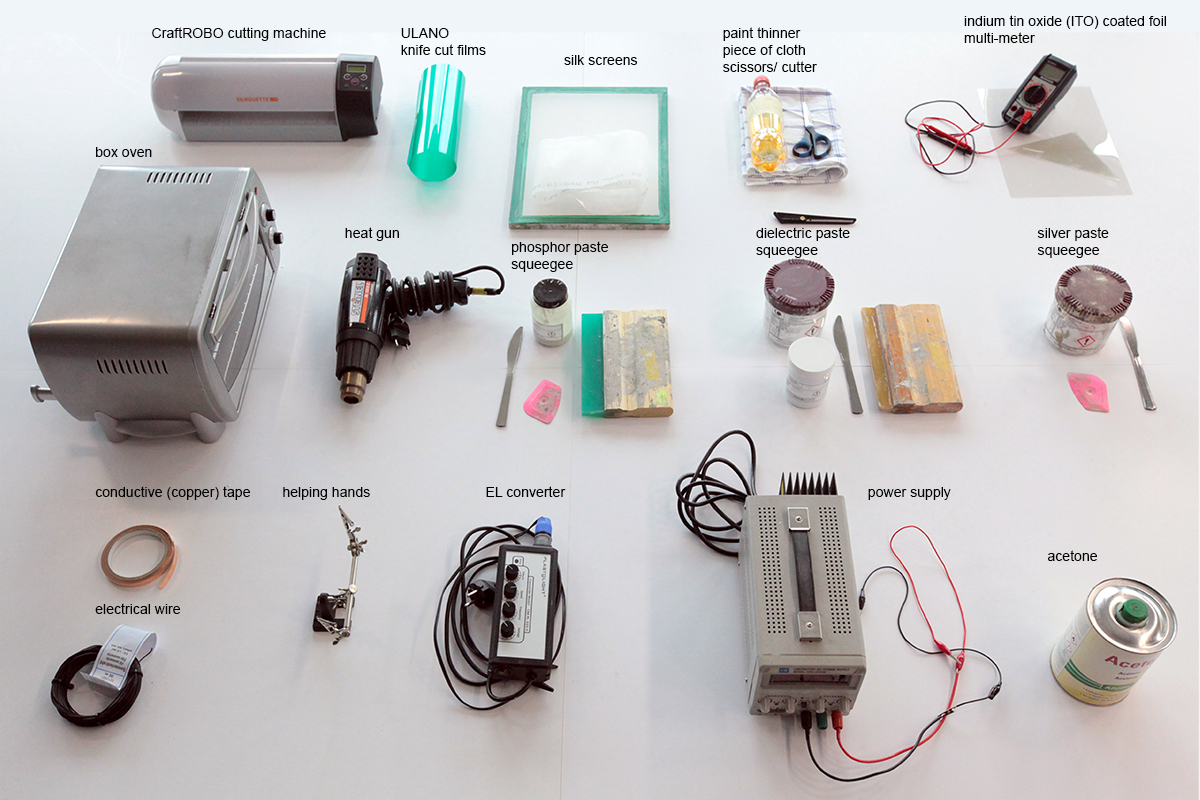
Materials and Tools
|
|
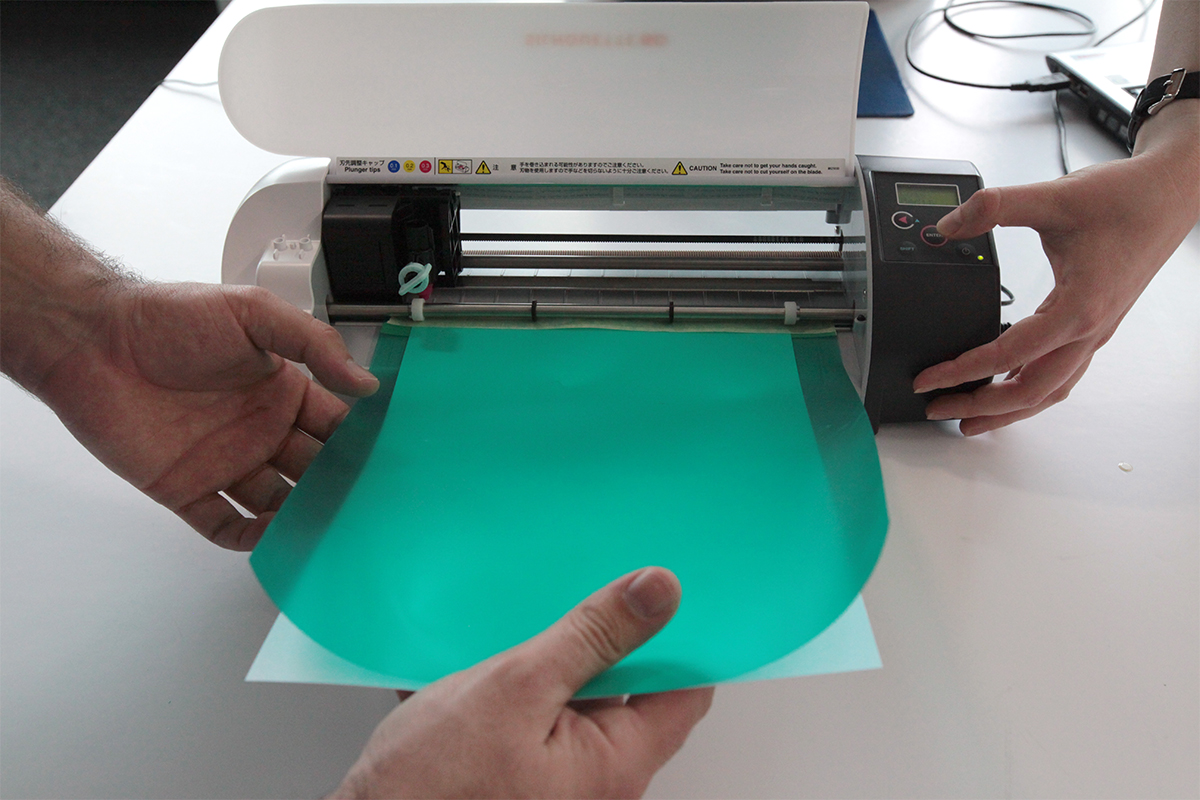
1. Create design and apply to Stencil Foil
Draw design on computer using a graphical program. Apply design to Knife Cut film with a cutting machine. It is important to create three different stencils, one for phosphor, one for dielectric and one for silver. The desired design only appears on the phosphor layer. The dielectric layer has to entirely cover the phosphor layer. The silver layer has to cover the phosphor layer but has to be smaller than the dielectric layer.

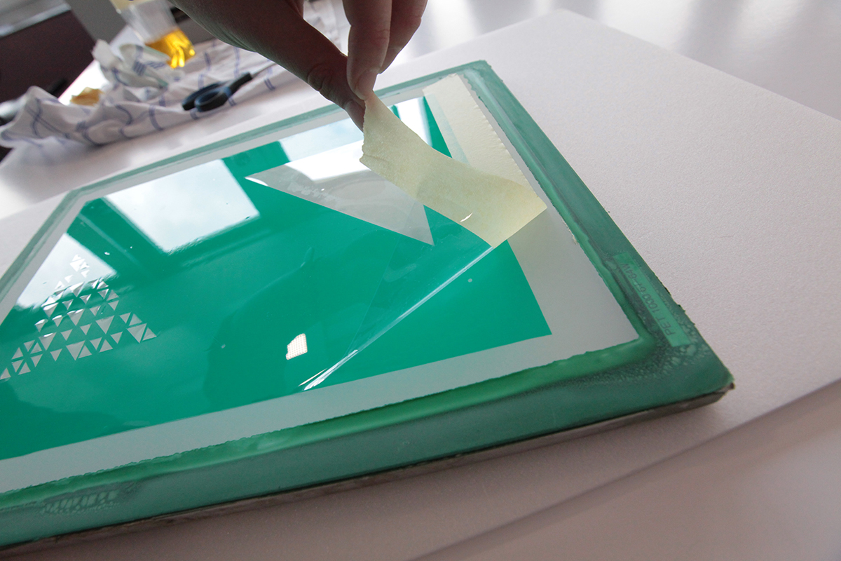
2. Apply knife cut film to Silk Screen
Remove cut out parts from the knife cut film. Fix film with “rough” side facing down onto silkscreen. Apply paint thinner to inner side of silkscreen by rubbing a soaked cloth onto the surface. After thinner has dissolved, remove plastic part of the film. For detailed instructions on how to work with the film, visit www.ulano.com/knifecut/stasharp.htm.


3. Prepare Work area
Mark perimeter of silk-screen onto white surface. Also mark outlines of designed shape four times, once for phosphor, twice for dielectric and once for silver.
4. Prepare Materials
Check electrical conductivity of both sides of ITO foil. Fix ITO foil with conductive side facing upwards onto previously marked first position (phosphor). Place silk screen with phosphor stencil above.


5. Print Phosphor
Apply thin line of phosphor paste on top end of shape. Press squeegee down firmly and print phosphor paste onto screen.
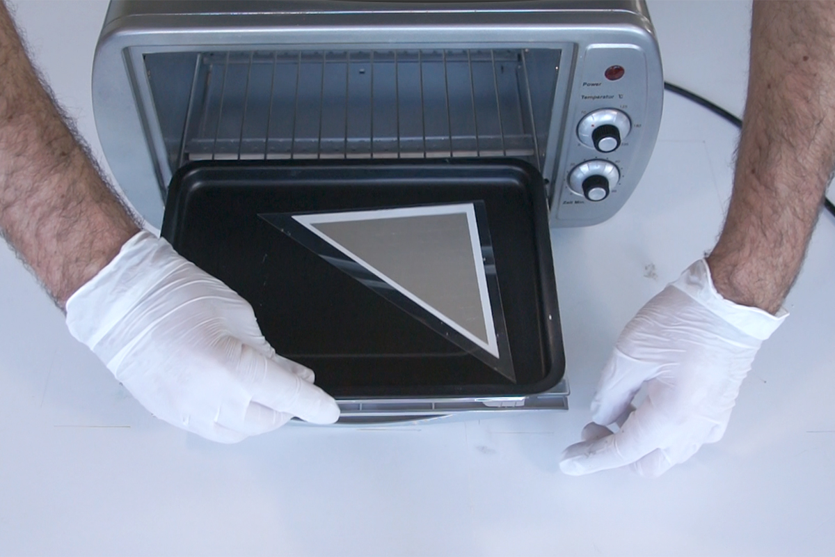
6. Dry and bake
Use heat gun to pre-dry the fresh print for about two minutes. Then bake inside box-oven for ten minutes at 130° C. Be careful when heating the foil, as too much heat will burn the material.


7. Print Dielectric
Place foil to dielectric position on work area. As in step 5, print thin layer of dielectric. Dry and bake the foil afterwards for 10 min at 130° C. Repeat step and print second layer of dielectric on top of first. These layer are the most important as they prevent the foil from shortening. Make sure to have no holes in the dielectric layer. (If necessary repeat this step until all holes are covered).
8. Print Silver
Place foil back onto work area, this time onto the silver position. As in steps 5 and 7, print thin layer of silver. Dry and bake foil for 10 minutes at 130° C.


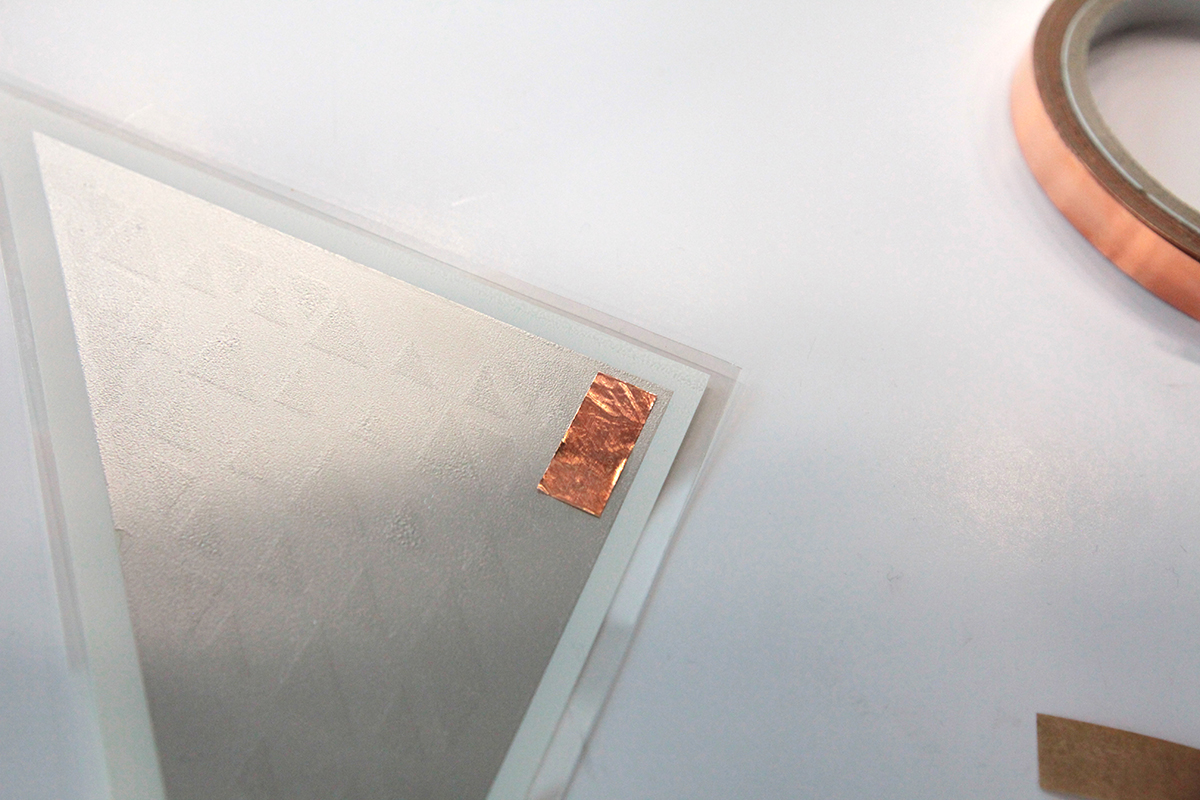
9. Add Connectors to active area
Cut four small strips of conductive tape and attach one to the silver layer. The component will work better if the tape sits in an area with phosphor on the other side. Use conductive tape again to fix an electrical wire on top of previously attached tape.
10. Add Connectors to conductive film
Repeat step 9 and add conductive tape and wire to ITO coated side of the foil. Make sure not to touch the silver layer.
11. Power
Connect component to EL converter.


12. Final dos and dont’s
- Double check your design! The display will light up only where all four layers overlap
- If the ITO and silver touch your display will short and not work
- Triple check which side of the ITO foil is conductive
- Use strong, confident strokes when screen printing to produce uniform layers
- Make sure each layer is completely dry before screening the next layer
- Be careful not to scratch your layers when connecting the leads
- The inverter produces a high voltage! Do not touch the two leads, it will sting
- If you want to keep excessive paste/ ink make sure to stir them from time to time